IBM has unveiled the world’s first 2 nm chip, built at its R&D facility in Albany, New York. The test chip features gate-all-around transistors built with IBM’s nanosheet technology. Overall, IBM says the new process technology will enable 2 nm chips to achieve 45% higher performance or 75% lower power consumption than state-of-the art 7 nm chips in production today.
IBM was also first to demonstrate 7 nm and 5 nm test chips. The test chip IBM showed today features about 50 billion transistors and uses nanosheet structures as part of a gate-all-around (GAA) transistor, the new transistor architecture heralded as the solution to the scaling limitations of its predecessor, the FinFET.
FinFET was commercially introduced by Intel for the 22 nm node in 2011. GAA transistors replace FinFET’s fin with three wires, surrounded on all sides by the gate material. Surrounding the channel material like this allows better electrostatic control which in turn enables extremely small gate dimensions.
With nanowires, the channel thickness (thickness of the wires) can be carefully controlled as the wires are epitaxially grown; FinFET channel thickness is not as tightly controllable due to the lithography and reactive ion etching processes used to create it.
While the first GAA transistors used a single nanowire, whose small dimensions reduce leakage but limit current and slow down switching, Samsung’s Multibridge Channel FET was the first to stack multiple wires vertically to allow more current to flow through the channel.

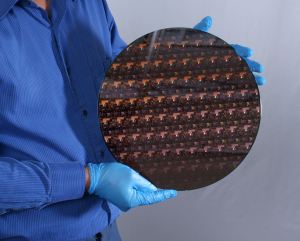
2 nm die on a 300 mm wafer from IBM’s research facility in Albany, New York (Source: IBM)
Expanding the wires into nanosheets increases the channel width while maintaining tight control over leakage current. Nanosheets can also be constructed with variable widths, restoring the flexibility that planar transistors had which FinFET took away. The width of the nanosheets can be widened to allow more current to flow or narrowed to save power.
Nanosheet-based processes are being readied by foundries including TSMC for the 3 nm node.
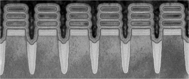
In IBM’s 2 nm chip, each transistor has three stacked nanosheets with 40 nm width and 5 nm height (5 nm, for reference, is about the same thickness as two strands of DNA). The transistors’ pitch is 44 nm and their gate length is 12 nm.
Note that the name “2 nm” does not relate to any particular size of any feature on the chip; the name of the process node is intended to reflect equivalent performance of a planar transistor with that feature size.
IBM highlighted several key technologies which have allowed miniaturization of the nanosheet transistor to this point. One is the use of bottom dielectric isolation — this eliminates leakage current between nanosheets and the bulk wafer. This reduction in leakage is required to scale the gate down to 12 nm. A second-generation inner space dry process is used to precisely control the size of the gate; this is based on IBM’s isotropic dry etch technique. There is also a novel multi-threshold-voltage scheme which enables threshold voltage control across the entire range of applications, from mobile to high-end server chips.
Crucially, this chip is the first to use extreme-ultraviolet lithography (EUV) for front-end of line (FEOL) processes. EUV is already in use for middle and back end of line processes, but this 2 nm chip is the first to use it for critical features such as the nanosheet and gate. It is this technology that enables the variable sheet width for designers of anywhere between 15 and 70 nm.

A row of 2 nm nanosheet transistors. The nanosheets are the three stacked sheets on top of each device. Each sheet is just 5 nm thick (Source: IBM)
The new 2 nm process node will be used for practically every application, spanning mobile electronics to high end servers and high-performance computing (HPC). This includes AI, 5G, 6G, autonomous systems and quantum computing. It will of course also be used for IBM’s own IBM Power Systems and IBM Z platforms, though these devices will continue to be manufactured by IBM’s manufacturing partner, Samsung.
The technology developments leading to today’s 2 nm chip are the result of years of work by IBM and its partners in the IBM Research Ecosystem. This now includes Intel, who recently joined the ecosystem after announcing it would double down on its own foundry business. IBM would not be drawn on whether Intel will use this technology for its own future 2 nm node, but it seems likely.
Of course, there is an awful lot of work to do before the technology that has created this test chip is ready for production, including ramping yield and working on device designs. IBM expects 2 nm foundry technology based on this work to go into production towards the end of 2024.
Sources: eetimes.com; newsroom.ibm.com
